Figure
1.
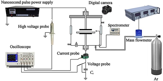
Experimental setup and measurement system.
| Citation: |
Wenhao ZHOU, Dongxuan ZHANG, Xiaohui DUAN, Xi ZHU, Feng LIU, Zhi FANG. Effect of dielectric material on the uniformity of nanosecond pulsed dielectric barrier discharge[J]. Plasma Science and Technology, 2024, 26(9): 094008. DOI: 10.1088/2058-6272/ad5fe6

|
Dielectric barrier discharge (DBD) is considered as a promising technique to produce large volume uniform plasma at atmospheric pressure, and the dielectric barrier layer between the electrodes plays a key role in the DBD processes and enhancing discharge uniformity. In this work, the uniformity and discharge characteristics of the nanosecond (ns) pulsed DBD with dielectric barrier layers made of alumina, quartz glass, polycarbonate (PC), and polypropylene (PP) are investigated via discharge image observation, voltage-current waveform measurement and optical emission spectral diagnosis. Through analyzing discharge image by gray value standard deviation method, the discharge uniformity is quantitatively calculated. The effects of the space electric field intensity, the electron density (Ne), and the space reactive species on the uniformity are studied with quantifying the gap voltage Ug and the discharge current Ig, analyzing the recorded optical emission spectra, and simulating the temporal distribution of Ne with a one-dimensional fluid model. It is found that as the relative permittivity of the dielectric materials increases, the space electric field intensity is enhanced, which results in a higher Ne and electron temperature (Te). Therefore, an appropriate value of space electric field intensity can promote electron avalanches, resulting in uniform and stable plasma by the merging of electron avalanches. However, an excessive value of space electric field intensity leads to the aggregation of space charges and the distortion of the space electric field, which reduce the discharge uniformity. The surface roughness and the surface charge decay are measured to explain the influences of the surface properties and the second electron emission on the discharge uniformity. The results in this work give a comprehensive understanding of the effect of the dielectric materials on the DBD uniformity, and contribute to the selection of dielectric materials for DBD reactor and the realization of atmospheric pressure uniform, stable, and reactive plasma sources.
Dielectric barrier discharge (DBD) can generate large volume non-equilibrium plasma at atmospheric pressure, which is characterized by high electron temperature, low gas temperature, large plasma volume and good uniformity [1–3]. The dielectric barrier layer(s) between electrodes is critical important to keep DBD plasma in good uniformity by limiting discharge current and preventing arc formation [4]. Therefore, DBD has broad application prospects in various fields, including material surface treatment [5, 6], ozone synthesis [7, 8], environmental protection [9, 10], and plasma biomedicine [11, 12]. To treat the material surface more evenly and further improve the energy efficiency of DBD, it is important to enhance the discharge uniformity of DBD further. The most common strategies to enhance the discharge uniformity are the promotion of the seed electron production, and the reduction of the space electric field distortion and the breakdown voltage [13]. These measures all serve to prevent excessive discharge intensity, thereby averting the formation of filamentary streamer discharges. Therefore, more efforts have been devoted to obtaining uniform DBD by selecting power supplies [14], working gases [15] and dielectric materials [16], and optimizing electrode structures [17] and operation conditions [18]. Fan et al established a bipolar pulse power supply through electrode optimization, using the charged particles generated by dielectric surface pre-ionization to enhance discharge uniformity [19]. Research by Guo et al indicated that appropriately increasing the flow rate can improve discharge uniformity [20]. The gas flow can mitigate the electron memory effect and reduce the likelihood of filamentary discharge channels forming. Among them, the different dielectric materials for dielectric barrier layers between electrodes have different relative permittivities, and surface physical and chemical properties, and can efficiently influence the space electric field intensity and the second electron generation near dielectric plate, which increases attention on the influence of dielectric materials on discharge uniformity [21–23].
Most of the efforts focus on the measurement of the DBD characteristics and the optimization of the DBD application effects with different dielectric materials. Ran et al investigated the impact of surface morphology on the air DBD mode in different dielectric materials (quartz and alumina) and found that as the surface roughness increased, there was a noticeable transition between the discharge modes [24]. Luo et al investigated the impact of dielectric surface morphology on discharge characteristics by comparing quartz and special ceramics as dielectric materials, revealing that shallow traps on the dielectric surface facilitate the generation of seed electrons for uniform discharge [25]. Ozkan et al conducted a study on the mechanisms of the influence of dielectric materials (alumina, pyrex, mullite and quartz) on the coaxial DBD mode and CO2 conversion through electrical characterization. The research revealed that higher effective plasma voltage in quartz is conducive to enhancing CO2 conversion efficiency [26]. Liu et al explored the influence of dielectric materials (quartz, alumina, and zirconia) on the characteristics of CO2 discharge and conversion in a planar DBD reactor. The results indicate that materials with higher relative permittivity exhibit elevated discharge intensity and enhanced CO2 conversion rates [27]. Teranishi et al studied the electrical properties and ozone generation characteristics of DBD under different dielectric materials, revealing that high thermal conductivity materials effectively transfer the generated heat to the external environment [28]. Wang et al studied the impact of different dielectric materials on the removal efficiency of NO [29]. These findings have demonstrated that the dielectric materials are of great importance for the discharge characteristics and the application effects of DBDs. However, the functions of the dielectric materials participating in the DBD processes are more complex, especially in DBD pulsed by nanosecond (ns) pulses, which involve the fast spatiotemporal evolution of the space electric field, the seed electron production, the charge accumulation and decay on dielectric barrier layer surface [30–32]. The previous results are mostly observed in specific conditions and there is lack of the comprehensive studies on the mechanisms of the dielectric materials on DBD processes. It limits the development of uniform and reactive plasma sources at atmospheric pressure and the applications of DBD. To improve the discharge uniformity, the effects of the dielectric materials on the discharge processes should be investigated thoroughly.
In this work, the discharge images of the ns pulsed DBDs with different dielectric materials (alumina, quartz glass, polycarbonate (PC), and polypropylene (PP)) have been recorded for the investigation of the discharge uniformity. To analyze the effects of dielectric materials on the uniformity of ns pulsed DBD, the discharge voltage dropped on the gap space and the discharge current are calculated from the measured voltage-current waveforms, and are used to estimate the space electric field intensity and electron density (Ne). The emission spectra are measured, and the temporal distribution of Ne is also simulated with a one-dimensional fluid model. The effects of the surface roughness and the surface charge decay of the different dielectric materials on the discharge processes are also analyzed and discussed.
The experimental setup and measurement system used in this study are illustrated in figure 1. An ns pulse power supply (Xi’an Lingfengyuan HV-2015) is employed as the driving source for DBD. It features a voltage amplitude range from 0 to 15 kV, a frequency range from 0 Hz to 100 kHz, and a pulse width range of 50 ns to 1 ms. The rise and fall times can be adjusted within the range of 50–500 ns. For this experiment, the ns pulse power supply is configured with a fixed repetition frequency of 2.5 kHz, a pulse width of 1500 ns, and rise and fall times of 50 ns. The reactor made of stainless steel, is capable of being evacuated to keep the working gas purity. A parallel plate electrode with a diameter of 50 mm is placed at the center of the reactor. It is covered with a 2 mm thick, 80 mm diameter dielectric barrier layer with different dielectric materials of alumina, quartz glass, PC, and PP with 6.0, 3.7, 2.6 and 3.1 relative permittivity values. The gap distance is fixed as 1.5 mm during experiment.
The applied voltage and total current are measured using a Northstar PVM-5 high-voltage probe and a Pearson Electronics Inc. 2877 current coil. The voltage crossing over a 2.2 nF reference capacitance (Cr) in the grounding electrode side is measured using an LDP-6002 differential probe. The voltage-current waveforms are collected using an oscilloscope (Tektronix 3054). The optical emission spectrum is measured by an Ocean Optics HR4000CG-UV spectrometer (wavelength range 200–1100 nm, resolution 0.75 nm). The discharge image is captured by a Canon EOS 6D camera with an exposure time of 50 ms. The high-purity argon (99.999% purity) is used as working gas, and the flow rate is controlled by Sevenstar D08-4F mass flow meter at 1 L/min. During the experiment, the pressure inside the reactor is maintained at 1.01×10⁵ Pa at a room temperature of 25 °C.
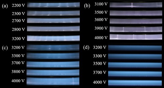
To investigate the effect of dielectric materials on the DBD uniformity, the discharge images of alumina, quartz glass, PP, and PC at different applied voltages are recorded and shown in figure 2. The change of the applied voltage can lead to the change of the space electrical field, which affects the discharge process and the discharge uniformity [33]. Due to the different relative permittivities of the investigated dielectric dielectrics, their initial discharge voltages are also different. To compare the discharge characteristics of different dielectrics, the voltage range is selected from the inception discharge voltage to the voltage at which discharge transitions to over-discharge, based on the actual discharge effects. From figure 2, it can be seen that as the increasing of the voltage, the discharge intensity is significantly enhanced. When alumina and quartz glass with high relative permittivity values are served as dielectric barrier layers as shown in figures 2(a) and (b), the uniform discharge can only be observed in a narrow voltage range. When PP and PC with low relative permittivity values are served as dielectric barrier layers as shown in figures 2(c) and (d), the uniform discharge can be observed in a large voltage range. The discharge mode can be determined qualitatively by eye from the discharge image. It is still important to analyze the DBD uniformity quantitatively. Some researchers had already used methods such as fast Fourier transform, spatial correlation functions, chi-squared tests, grayscale analysis, etc., to analyze discharge uniformity from discharge images [34, 35]. In our previous work [36], a gray value standard deviation (GVSD) method was developed for quantitative analysis of discharge uniformity, involving the conversion of discharge images into grayscale value and subsequent standard deviation calculation. First, the images captured from the central discharge region are converted to grayscale to obtain the gray values of the pixels on the 40 mm long horizontal line in the middle of the discharge area. Next, the pixel values along the centerline of the discharge space are extracted as the reference value xn. Using the average value xm of xn, the grayscale values are normalized, as shown in equation (1):
| ¯xn=xn−xmv, | (1) |
where xn represents the zero-mean normalized pixel value, v is the variance. For the evaluation of the discharge uniformity, the gradient value of ¯xn′ is obtained by the differentiation of xn. The standard deviation of ¯xn′, GVSD, is used to represent the uniformity of the discharge.
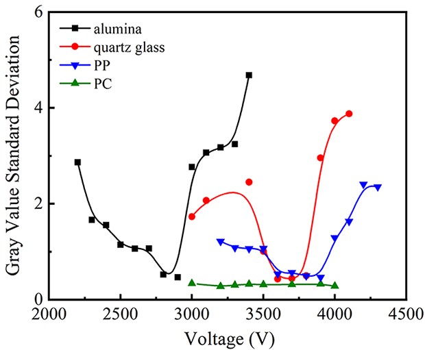
Figure 3 shows the corresponding GVSD values of the discharge images in figure 2. It is shown that the GVSD values for PC consistently remain at a low level, whereas only few conditions for alumina and quartz glass are below 1. This indicates that PC has good discharge uniformity, which is consistent with the results of the discharge images.
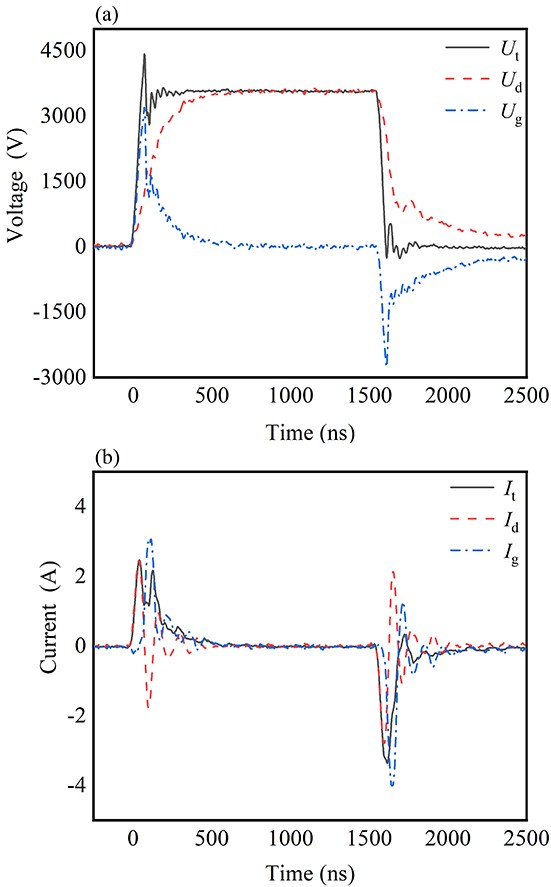
From the observed discharge images, it can be seen that the applied voltage affects the discharge uniformity significantly by the electric field in discharge space. For DBD, the applied voltage is applied on the dielectric barrier and the gas gap, and to accurately obtain the dynamic change process of voltage on the gas gap, it is necessary to separate the applied voltage (Ut) to obtain the applied voltage (Ud) on the dielectric barrier layer and the voltage (Ug) on the gas gap. Our research group previously used the method of series connection of sampling capacitors at the ground electrode for voltage separation [36, 37]. As the reference capacitor is a capacitive load, its voltage (Ur) should be proportional to the dielectric barrier layer voltage Ud. When the discharge is extinguished, nearly all of Ut is applied on dielectric barrier and Ug is close to 0. An appropriate coefficient can be selected to simulate Ud by multiplying with Ur. Ug can be obtained by subtracting Ud from Ut. For the measured total current (It), it is composed of the displacement current (Id) and the conduction current (Ig) in the gas gap. Id can be obtained by pumping reactor to vacuum or replace to extinguish discharge at the same Ut. Then, Id can be subtracted from the total current It to obtain Ig [37]. Figure 4 shows the separation of voltage-current waveforms of DBD with dielectric barrier layer of alumina.
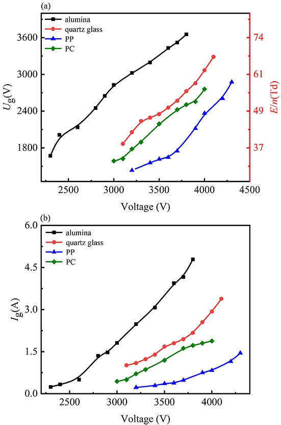
In previous studies, the pulse rise time has been identified as an important factor of achieving discharge uniformity [38]. The rate of pulse rise significantly affects Ug and the E/n, whereas the pulse fall time primarily concerns charge accumulation and does not impact critical parameters such as Ug. Therefore, this study only explores the effect of the discharge rise time on the discharge uniformity of different dielectric materials. It can be seen from figure 4(a) that on the voltage rising edge, Ug rises rapidly when Ut rises, which means most of voltage drops on the gas gap. Ud rises slowly and causes Id in figure 4(b). When the peak value of Ug reaches the threshold voltage, the breakdown occurs, which leads to the decrease of Ug and the appearance of Ig. With more charges accumulated on dielectric barrier layer surface, the reverse electric field by the accumulated charges distinguishes the discharge and most voltage drops on the dielectric barrier. On the voltage rising edge, with the rapidly drop of Ut, the reverse electric field reaches the threshold voltage, the reverse discharge occurs as the reverse peaks of Ug and Ig shown in figures 4(a) and (b). Figure 5 shows the peak values of Ug, which can estimate the reduced electric field E/n in space, and Ig on the voltage rising edge of the ns pulsed DBDs of different applied voltages with different dielectric materials. It can be seen that at same Ut, Ug of ns pulsed DBD with dielectric barrier layer of alumina is always the highest compared with the others, which results in a high space electric field intensity and causes filament discharge more easily. The ns pulsed DBDs with dielectric barrier layers of PC and PP have low Ug, which favors the generation of uniform discharge.
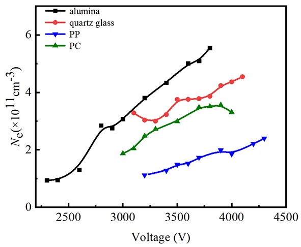
The different values of Ug in the ns pulsed DBDs with dielectric barrier layers at same Ut are caused by the different relative permittivity values. Alumina has the highest relative permittivity value, 6.0, and more voltage drops in space. While, PC and PP have low relative permittivity values, 2.6 and 3.1, and little voltages drop in space. As the relative permittivity increases, there is a corresponding increase in E/n, which leads to a higher ionization rate, a higher electron drift velocity, a higher Ne and a higher value of Ig. At same Ug, a higher Ne would easily lead to space electric field distortion and result in filament discharge. Ne can be estimated from the equation (2) [36]:
| IgS=eNeVdrift, | (2) |
where S is the area of discharge, e is the elementary charge, Vdrift is the drift velocity of electron, which is defined as the equation (3):
| Vdrift=μeE, | (3) |
where µe is the electron mobility, which can be obtained by BOLSIG+ code with the corresponding E/n [37, 39]. The calculated values of Ne of the ns pulsed DBDs with different dielectric materials are given in figure 6. It can be seen that at the same Ut, there is a significant difference in the values of Ne of the ns pulsed DBDs with different dielectric materials. From the electrical characteristics’ measurement, the E/n and Ne are the important factors affecting the discharge uniformity of the DBDs with different dielectric materials.
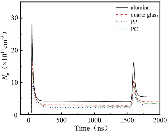
The values of Ne given in figure 6 are the peak values. The time resolved Ne of the ns pulsed DBDs with different dielectric materials can be calculated by a one-dimensional plasma fluid model with continuity equation and momentum equation [40], which is a self-programmed FORTRAN code and is reported in our previous work [33]. Figure 7 shows the time resolved Ne of the ns pulsed DBDs with dielectric materials of alumina, quartz, PP, and PC at 3700 V, which shows the ns pulsed DBDs with a higher relative permittivity dielectric material obtaining a higher Ne at both the rising and falling edges.
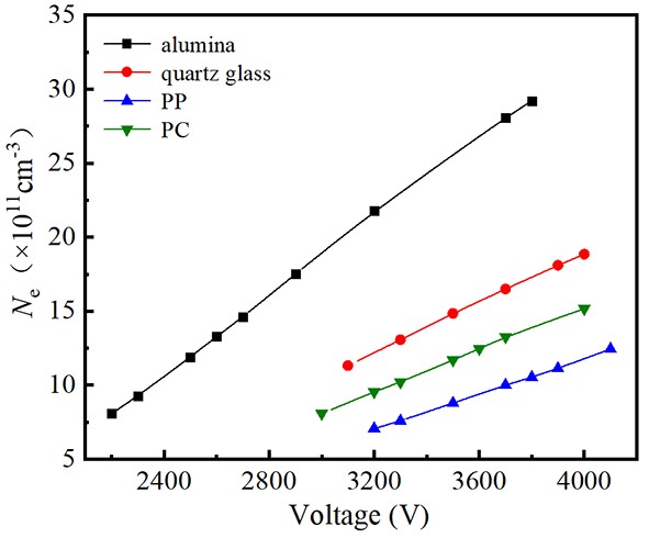
Figure 8 also shows the peak values of Ne of the ns pulsed DBD with different dielectric materials at different voltages. Compared with figure 6, the tendencies of the peak values of Ne are the same with the highest Ne of the ns pulsed DBD with dielectric material of alumina and the lowest Ne of the ns pulsed DBD with dielectric material of PC. However, the simulation results are several times higher of the experimental calculated results, which are caused by the error in the calculation process and the inaccurate coefficients. However, due to the overestimation of the initial density of atmospheric molecules and inaccuracies in the secondary electron emission coefficient during the simulation calculations, the simulation results are several times higher than the experimental results.
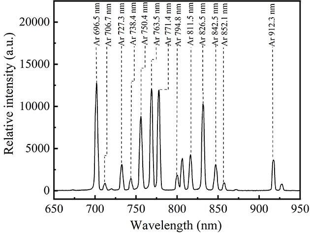
The reactive species in Ar plasma are mainly excited argon atom Ar*, metastable argon atom Arm, argon atom ion Ar+, and argon molecular ion Ar2+ [41], but only a few of them can be observed by the optical emission spectra measurement. Figure 9 shows a typical emission spectrum of the ns pulsed DBD with alumina as a dielectric barrier layer at 3.5 kV, which are mainly composed of Ar (2p–1s) emission lines.
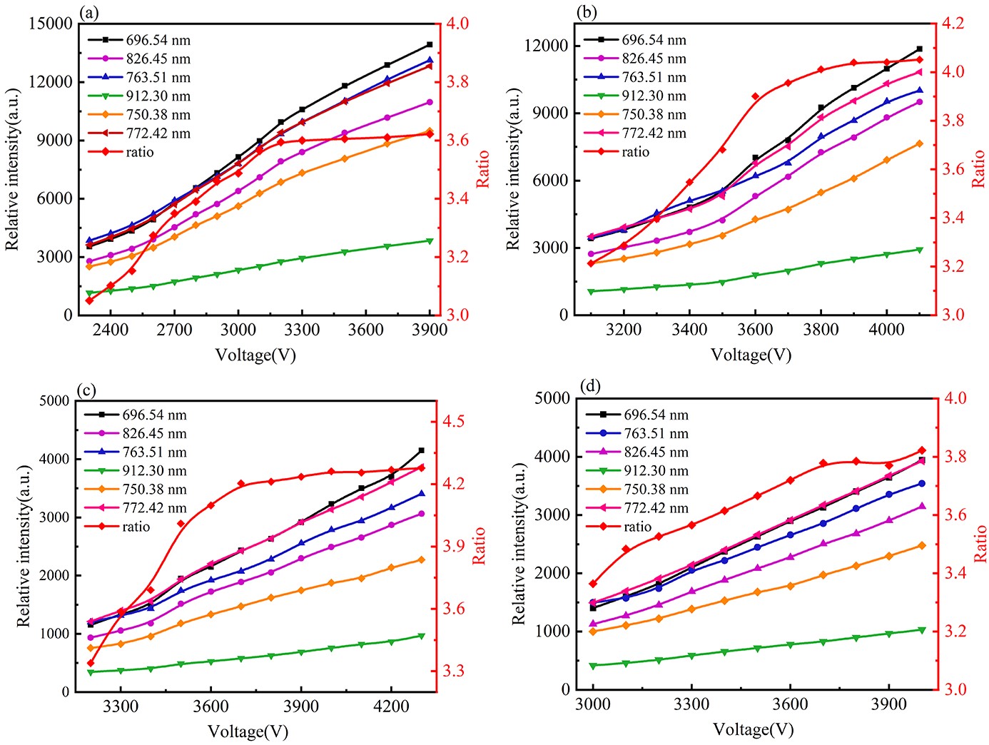
Figure 10 shows the emission intensities of Ar emission lines and the intensity ratio of Ar (696.5 nm) and Ar (912.3 nm) at different voltages of the ns pulsed DBDs with the dielectric barrier layers of alumina, quartz glass, PP, and PC. It can be seen that the ns pulsed DBD with dielectric material of alumina has the highest emission intensities, which is consistent with the electrical characteristics results. The high Ug and Ig result in the high densities of reactive species. For the ratio of Ar (696.5 nm) and Ar (912.3 nm), it can indicate the trend of the electron energy, Te [42–46]. That is because the emission intensity I of Ar excited by direct electron collisional excitation can be given as follows:
| I∝CλAτnArNek, | (4) |
where Cλ represents the spectral response of the optical measurement system, A stands for the Einstein coefficient, τ is the effective lifetime, nAr is the number density of ground-state Ar, and k represents the excitation rate (determined by Te). The intensity ratio of Ar emission lines, I1/I2, is proportional to the ratio of excitation rates, k1/k2, as follows [37, 46]
| I1I2=Cλ1A1τ1k1Cλ2A2τ2k2, | (5) |
| k1k2=Cλ2A2τ2I1Cλ1A1τ1I2=CI1I2. | (6) |
Therefore, I1/I2 can reflect the trend of k1/k2 changes, which characterizes the changes in Te. In this study, the emission lines of Ar (696.5 nm) and Ar (912.3 nm) with excitation energies of 13.3 eV and 12.9 eV are selected to calculate I1/I2. From figure 10, it can be seen that the ratios of I1/I2 of the ns pulsed DBDs with the dielectric barrier layers of alumina, quartz glass, and PP increase firstly and then saturate in the studied voltage, while the ratio of I1/I2 of the ns pulsed DBD with the dielectric barrier layer of PC increases almost linearly. It is because the discharge mode changes from uniform to filament, which costs energy in the filamentary channels and saturates or even reduces Te. The ns pulsed DBD with the dielectric barrier layer of PC stays in uniform mode in the studied voltage range and the increased input energy increases its Te.
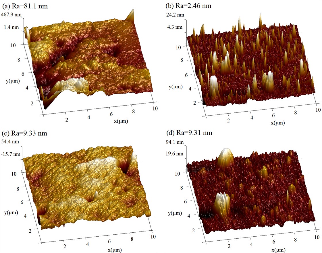
The discharge uniformity is not only determined by the space electric field and the space particles but also determined by the materials properties, especially the surface properties, which affects second electron emission and charge dissipation [47, 48]. Hence, it is necessary to characterize the surface characteristics of the dielectric materials and explore their effects on the discharge uniformity. The atomic force microscope (AFM) images of the dielectric materials used for the ns pulsed DBDs are measured and depicted in figure 11. The average surface roughness (Ra) of alumina is the highest with a value of 81.1 nm. The uneven surface is prone to generate excessively strong localized electric fields, thereby affecting discharge uniformity. The values of Ra of quartz, PP, and PC are less than 10 nm. This lower roughness is advantageous for achieving a uniform distribution of the electric field within the discharge gap, consequently enhancing discharge performance.
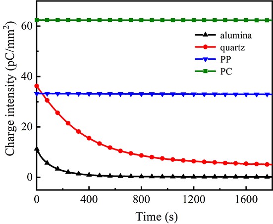
The charge dissipation on the material surface can supply free electrons for next discharge. PC and PP are the electret materials with shallow wells to trap electrons, which are considered important to generate uniform discharge [47–50]. Therefore, the charge dissipation rates of alumina, quartz glass, PP and PC are measured with the procedure by polarizing at 3000 V for 5 min and measuring the surface potential immediately after charging. The surface charge density of the dielectric materials with time is shown in figure 12.
From figure 12, it can be seen that the surface charge density of alumina and quartz glass decays fast after charging. After 1000 s, the surface charge density of alumina decreases to 0.26 pC/mm2, while that of quartz glass shows 7.22 pC/mm2. In contrast, the surface charge density of PP and PC shows minimal reduction. After 1000 s, the surface charge density of PP is 33.05 pC/mm2, while that of PC is 62.33 pC/mm2. It is concluded that PC and PP have more surface charges for next discharge, which lowers the discharge threshold voltage and the space electric field intensity. Therefore, the ns pulsed DBDs with the dielectric materials of PC and PP have better uniformity than those with the dielectric materials of alumina and quartz glass with lower Ug, lower Ig, and lower surface charge dissipation capability.
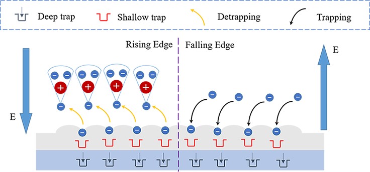
Figure 13 illustrates the effect of the dielectric material surface on the discharge. During the rising edge, charges trapped in shallow traps on the dielectric surface are released by the external electric field. These released charges provide additional seed electrons for the discharge, facilitating electron avalanche formation, reducing the breakdown voltage of the air gap, and weakening the discharge intensity, which promotes uniform discharge. During the falling edge, electrons, influenced by the electric field, move to the dielectric surface and are captured by shallow traps, where they are stored as secondary seed electrons for the next discharge. Deep traps, requiring more energy, cannot capture a significant amount of charge. From this, it is evident that electret materials such as PP and PC, which can store more electrons on their surfaces, provide more seed electrons at the start of the next discharge cycle. This facilitates electron avalanche formation, resulting in a lower breakdown voltage of the air gap and maintaining discharge intensity at an appropriate level. It avoids electric field distortion and promotes discharge uniformity.
In this work, the effects of dielectric materials on the uniformity of ns pulsed DBD are investigated by electrical and optical diagnosis. It is found that the uniformity of DBDs with PC and PP dielectric barriers are better than those with alumina and quartz glass from observation of the discharge images and calculation of the GVSD values. With voltage-current waveform separation processing, the voltage on the gas gap Ug and the conduction current Ig are obtained from applied voltage Ug and total current It. At same Ut, Ug of DBDs with alumina and quartz glass are higher than those with PC and PP due to larger relative permittivity values. A higher Ug results in a higher space electric field intensity and E/n, causing higher intensities of space charges, active species, and then higher Ig, which are confirmed by the one-dimensional fluid model simulation results and the emission spectra measurements. A higher space electric field intensity of DBDs with alumina and quartz glass promotes the formation of filaments in discharge space. The low discharge thresholds in space of DBDs with PC and PP are mainly due to their electret properties with more surface charges supplying for successive discharge. From the surface charge measurement of the four dielectric materials, it is found that the surface charge densities of PP and PC are 33.05 pC/mm2 and 62.33 pC/mm2 after 1000 s, which provides seed electrons and lowers the discharge threshold.
This work was supported by National Natural Science Foundation of China (Nos. 52037004 and 52177148) and Postgraduate Research & Practice Innovation Program of Jiangsu Province (No. KYCX23_1449).
| [1] |
Shcherbanev S A et al 2019 Plasma Sources Sci. Technol. 28 065013 doi: 10.1088/1361-6595/ab2230
|
| [2] |
Cui W S et al 2021 Plasma Sci. Technol. 23 075402 doi: 10.1088/2058-6272/abf9fd
|
| [3] |
Xu Q N et al 2023 Vacuum 207 111688 doi: 10.1016/j.vacuum.2022.111688
|
| [4] |
Moussaoui A et al 2017 J. Electrostat. 87 102 doi: 10.1016/j.elstat.2017.04.005
|
| [5] |
Niu Q et al 2017 Fuel Process. Technol. 156 310 doi: 10.1016/j.fuproc.2016.09.013
|
| [6] |
Krawczyk K et al 2023 Materials 16 2973 doi: 10.3390/ma16082973
|
| [7] |
Pekárek S et al 2020 J. Phys. D: Appl. Phys. 53 275203 doi: 10.1088/1361-6463/ab831f
|
| [8] |
Gou X X et al 2023 Vacuum 212 112047 doi: 10.1016/j.vacuum.2023.112047
|
| [9] |
Yoshida K 2019 IEEE Trans. Ind. Appl. 55 5261 doi: 10.1109/TIA.2019.2924879
|
| [10] |
Li Z et al 2023 Environ. Sci. Pollut. Res. 30 66291 doi: 10.1007/s11356-023-27125-8
|
| [11] |
Zhao L X et al 2023 Plasma Chem. Plasma Process. 43 1567 doi: 10.1007/s11090-023-10384-1
|
| [12] |
Nawaz M I et al 2023 Environ. Res. 237 117015 doi: 10.1016/j.envres.2023.117015
|
| [13] |
Yu S et al 2016 Phys. Plasmas 23 023510 doi: 10.1063/1.4942225
|
| [14] |
Yuan H et al 2017 Plasma Sci. Technol. 19 125401 doi: 10.1088/2058-6272/aa8766
|
| [15] |
Pan J et al 2015 IEEE Trans. Plasma Sci. 43 557 doi: 10.1109/TPS.2014.2385877
|
| [16] |
Jiang S et al 2021 Plasma Sci. Technol. 23 125404 doi: 10.1088/2058-6272/ac2b11
|
| [17] |
Liu S et al 2023 Vacuum 209 111793 doi: 10.1016/j.vacuum.2022.111793
|
| [18] |
Zhang S et al 2019 J. Appl. Phys. 125 113301 doi: 10.1063/1.5052697
|
| [19] |
Fan R et al 2020 Phys. Plasmas 27 083508 doi: 10.1063/5.0007662
|
| [20] |
Guo H F et al 2020 Phys. Plasmas 27 023519 doi: 10.1063/1.5117885
|
| [21] |
Yao J X et al 2023 Appl. Phys. Lett. 122 082905 doi: 10.1063/5.0139247
|
| [22] |
Ma X Q et al 2021 J. Phys. D: Appl. Phys. 54 505204 doi: 10.1088/1361-6463/ac22d5
|
| [23] |
Bian D L et al 2018 J. Appl. Phys. 124 183301 doi: 10.1063/1.5049463
|
| [24] |
Ran J X et al 2021 IEEE Trans. Plasma Sci. 49 214 doi: 10.1109/TPS.2020.3043580
|
| [25] |
Luo H Y et al 2017 IEEE Trans. Plasma Sci. 45 749 doi: 10.1109/TPS.2017.2679210
|
| [26] |
Ozkan A et al 2016 Plasma Sources Sci. Technol. 25 045016 doi: 10.1088/0963-0252/25/4/045016
|
| [27] |
Liu C Y et al 2023 Plasma Sources Sci. Technol. 32 025011 doi: 10.1088/1361-6595/acb816
|
| [28] |
Teranishi K et al 2009 Plasma Sources Sci. Technol. 18 045011 doi: 10.1088/0963-0252/18/4/045011
|
| [29] |
Wang T et al 2012 Plasma Chem. Plasma Process. 32 1189 doi: 10.1007/s11090-012-9399-3
|
| [30] |
Akishev Y et al 2011 Plasma Sources Sci. Technol. 20 024005 doi: 10.1088/0963-0252/20/2/024005
|
| [31] |
Suzuki S and Itoh H 2015 Plasma Sources Sci. Technol. 24 055016 doi: 10.1088/0963-0252/24/5/055016
|
| [32] |
Xu S W et al 2013 Phys. Plasmas 20 083515 doi: 10.1063/1.4819258
|
| [33] |
Zhang D X et al 2023 Plasma Sci. Technol. 25 114004 doi: 10.1088/2058-6272/acd83c
|
| [34] |
Wang Y Y et al 2021 Plasma Sources Sci. Technol. 30 075009 doi: 10.1088/1361-6595/abfbc6
|
| [35] |
Liu C, Dobrynin D and Fridman A 2014 J. Phys. D: Appl. Phys. 47 252003 doi: 10.1088/0022-3727/47/25/252003
|
| [36] |
Liu F et al 2021 J. Appl. Phys. 129 033302 doi: 10.1063/5.0031220
|
| [37] |
Liu F, Huang G and Ganguly B 2010 Plasma Sources Sci. Technol. 19 045017 doi: 10.1088/0963-0252/19/4/045017
|
| [38] |
Liu F et al 2023 Plasma Sci. Technol. 25 104001 doi: 10.1088/2058-6272/acd529
|
| [39] |
Lisovskiy V et al 2010 J. Phys. D: Appl. Phys. 43 385203 doi: 10.1088/0022-3727/43/38/385203
|
| [40] |
Barjasteh A and Eslami E 2016 Phys. Plasmas 23 033506 doi: 10.1063/1.4943407
|
| [41] |
Lee M H and Chung C W 2005 Phys. Plasmas 12 073501 doi: 10.1063/1.1935407
|
| [42] |
Tabaie S S, Iraji D and Amrollahi R 2020 Vacuum 182 109761 doi: 10.1016/j.vacuum.2020.109761
|
| [43] |
Siasko A et al 2023 Phys. Plasmas 30 033701 doi: 10.1063/5.0135329
|
| [44] |
Ran J X et al Diagnosis of the electron temperature in dielectric barrier discharge by optical emission spectroscopy In: Proceedings Qptical Design and Testing II Beijing, China: SPIE 2005, doi: 10.1117/12.571588
|
| [45] |
Li H and Xie M F 2013 Plasma Sci. Technol. 15 776 doi: 10.1088/1009-0630/15/8/11
|
| [46] |
Dedrick J et al 2011 J. Phys. D: Appl. Phys. 44 205202 doi: 10.1088/0022-3727/44/20/205202
|
| [47] |
Mitsuhashi K et al 2021 Plasma Sources Sci. Technol. 30 04LT02 doi: 10.1088/1361-6595/abefa7
|
| [48] |
Ambrico P F et al 2010 J. Phys. D: Appl. Phys. 43 325201 doi: 10.1088/0022-3727/43/32/325201
|
| [49] |
Zhang S et al 2019 Molecules 24 3933 doi: 10.3390/molecules24213933
|
| [50] |
Li T et al 2022 Plasma Sources Sci. Technol. 31 055016 doi: 10.1088/1361-6595/ac676e
|
| 1. | Yang, X., Keener, K.M., Cheng, J.-H. Enhancing the discharge uniformity of atmospheric pressure DBD cold plasma for food efficient microbial inactivation. Journal of Food Engineering, 2025. DOI:10.1016/j.jfoodeng.2024.112389 | |
| 2. | Zhou, Y., Fang, Z., Zhang, Y. et al. Surface Hydrophilic Modification of Polypropylene by Nanosecond Pulsed Ar/O2 Dielectric Barrier Discharge. Materials, 2025, 18(1): 95. DOI:10.3390/ma18010095 | |
| 3. | Ran, J., Chen, Q., Zhou, Y. et al. Comparative Study on Surface Modification of Polyethylene Terephthalates by Four Discharge Modes. Plasma Processes and Polymers, 2025. DOI:10.1002/ppap.70023 | |
| 4. | Zhang, L., Zhang, Z., Zhang, D. et al. Hydrophilic surface modification of polypropylene by AC-DBD and NS-DBD. Surfaces and Interfaces, 2024. DOI:10.1016/j.surfin.2024.104093 | |
| 5. | Liu, F., Li, S., Zhao, Y. et al. The effect of pulse voltage rise rate on the polypropylene surface hydrophilic modification by ns pulsed nitrogen DBD. Plasma Science and Technology, 2023, 25(10): 104001. DOI:10.1088/2058-6272/acd529 | |
| 6. | Liu, F., Wang, Y., Wang, W. et al. Generation of the high power by a coaxial dielectric barrier discharge with a perforated electrode in atmospheric pressure air. Physics of Plasmas, 2023, 30(9): 093508. DOI:10.1063/5.0160137 | |
| 7. | Liang, C., Liu, Z., Sun, B. et al. Improvement in discharge characteristics and energy yield of ozone generation via configuration optimization of a coaxial dielectric barrier discharge reactor. Chinese Journal of Chemical Engineering, 2023. DOI:10.1016/j.cjche.2022.11.016 | |
| 8. | Zhu, Y., Huang, J., Guo, S. et al. Enhancement of Hydrophobic Properties of Epoxy Resin by Large Area Dielectric Barrier Discharge Plasma Treatment Device. 2023. DOI:10.1109/ICEMPE57831.2023.10139490 | |
| 9. | Li, S., Li, J., Fu, Y. et al. Interaction between plasma jet and silicone rubber covered by porous inorganic contaminants: Surface hydrophobicity or hydrophilicity?. High Voltage, 2022, 7(6): 1023-1033. DOI:10.1049/hve2.12122 | |
| 10. | Chen, J., Zhang, D., Ding, Y. et al. Effects of Pulse Repetition Frequency and Voltage Slew Rate on the Uniformity of Air Dielectric Barrier Discharge. 2022. DOI:10.1109/ICHVE53725.2022.10014478 | |
| 11. | Li, S., Ding, Y., Zhao, Y. et al. Effect of pulse voltage slew rate on the uniformity of polypropylene surface hydrophilic modification by nanosecond pulsed dielectric barrier discharge. Annual Report - Conference on Electrical Insulation and Dielectric Phenomena, CEIDP, 2022. DOI:10.1109/CEIDP55452.2022.9985297 | |
| 12. | Shi, Y., Lu, Y., Cai, Y. et al. Experimental study on the parameter optimization and application of a packed-bed dielectric barrier discharge reactor in diesel particulate filter regeneration. Plasma Science and Technology, 2021, 23(11): 115505. DOI:10.1088/2058-6272/ac1dfd | |
| 13. | Guo, Y., Liu, P., Zhang, L. et al. Disinfection of Escherichia coli in ice by surface dielectric barrier discharge plasma. Applied Physics Letters, 2021, 119(9): 090601. DOI:10.1063/5.0064020 | |
| 14. | Lu, N., Liu, N., Hui, Y. et al. Characterization of highly effective plasma-treated g-C3N4 and application to the photocatalytic H2O2 production. Chemosphere, 2020. DOI:10.1016/j.chemosphere.2019.124927 | |
| 15. | Zhao, L., Liu, W., Xu, M. et al. Study on atmospheric air glow discharge plasma generation based on multiple potentials and aramid fabric surface modification. Plasma Processes and Polymers, 2019, 16(12): 1900114. DOI:10.1002/ppap.201900114 | |
| 16. | Guo, L.-T., Dong, L.-F., Wang, Z.-Y. et al. White Eyes Superlattice Concentric Ring Luminescent Pattern in Dielectric Barrier Discharge | [介质阻挡放电中白眼超点阵同心圆环发光斑图]. Faguang Xuebao/Chinese Journal of Luminescence, 2019, 40(10): 1311-1317. DOI:10.3788/fgxb20194010.1311 |
Supported by: Beijing Renhe Information Technology Co., Ltd. 
 DownLoad: