| Citation: |
Peng ZHANG, Ruvarashe F DAMBIRE. Competitive effect between roughness and mask pattern on charging phenomena during plasma etching[J]. Plasma Science and Technology, 2022, 24(3): 035502. DOI: 10.1088/2058-6272/ac48df

|
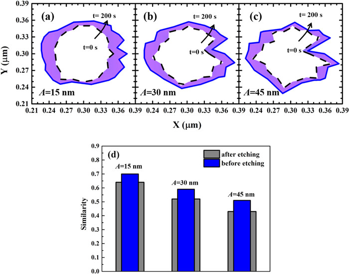
In the plasma etching process, the edge roughness and mask pattern usually play a significant role in the deformation of holes under the influence of the charging effect. The competitive effect between these two factors has been investigated, focusing on the surface charging in a hexagonal array, with various values of roughness parameters (amplitude (A) and wavelength (W)) and distances between holes (L). A series of classical particle dynamic simulations of surface charging, surface etching and profile evolution were used to investigate the effect of roughness and pattern on charging. This study showed that various roughness and patterns (represented by different values of L) can significantly influence surface distributions of the electric-field (E-field) and the etching rates on the mask surface. The simulations also showed that (1) the shape of the pattern array influences the mask hole profile during the etching process, i.e. a hexagonal array pattern tends to deform the profile of a circular mask hole into a hexagonal hole; (2) pattern roughness is aggravated during the etching process. These factors were found to be significant only at a small feature pitch and may be ignored at a large feature pitch. Possible mechanisms of these results during the etching process are discussed. This work sheds light on the ways to maintain pattern integrity and further improve the quality of the pattern transfer onto the substrate.
This work was supported by Youth Project of Science and Technology Research Program of Chongqing Education Commission of China (No. KJQN201901407), the start-up research funding of Yangtze Normal University, China (No. 2017KYQD113), 2017 Youth Research Talent Supporting Program, China (No. 2017QNRC18).
| [1] |
Wu B Q, Kumar A and Pamarthy S 2010 J. Appl. Phys. 108 051101 doi: 10.1063/1.3474652
|
| [2] |
Abe H, Yoneda M and Fujiwara N 2008 Jpn. J. Appl. Phys. 47 1435 doi: 10.1143/JJAP.47.1435
|
| [3] |
Donnelly V M and Kornblit A 2013 J. Vac. Sci. Technol. A 31 050825 doi: 10.1116/1.4819316
|
| [4] |
Kanarik K J 2012 Solid State Technol. 55 14
|
| [5] |
Ryu H K et al 2003 Electrochem. Solid-State Lett. 6 C126 doi: 10.1149/1.1594412
|
| [6] |
Thomas D J et al 1989 J. Vac. Sci. Technol. B 8 516 doi: 10.1116/1.585053
|
| [7] |
Sung K T and Pang S W 1994 Jpn. J. Appl. Phys. 33 7112 doi: 10.1143/JJAP.33.7112
|
| [8] |
Sun X Q et al 2012 Thin Solid Films 520 5946 doi: 10.1016/j.tsf.2012.05.016
|
| [9] |
Tsougeni K et al 2018 Colloids Surf. B Biointerfaces 165 270 doi: 10.1016/j.colsurfb.2018.02.055
|
| [10] |
Tsougeni K et al 2009 Langmuir 25 11748 doi: 10.1021/la901072z
|
| [11] |
Palumbo F et al 2011 Plasma Process. Polym. 8 118 doi: 10.1002/ppap.201000098
|
| [12] |
Li Y P et al 2012 Surf. Coat. Technol. 206 4952 doi: 10.1016/j.surfcoat.2012.05.120
|
| [13] |
Vourdas N et al 2008 Microelectron. Eng. 85 1124 doi: 10.1016/j.mee.2007.12.032
|
| [14] |
Papageorgiou D P et al 2013 Microfluid. Nanofluidics 14 247 doi: 10.1007/s10404-012-1043-2
|
| [15] |
Zhang P et al 2013 Plasma Sci. Technol. 15 570 doi: 10.1088/1009-0630/15/6/15
|
| [16] |
Negishi N et al 2017 J. Vac. Sci. Technol. B 35 051205 doi: 10.1116/1.4998943
|
| [17] |
Radjenovic B M, Radmilovic-Radjenovic M D and Petrovic Z L 2008 IEEE Trans. Plasma Sci. 36 874 doi: 10.1109/TPS.2008.920886
|
| [18] |
Satoshi H et al 1997 Jpn. J. Appl. Phys. 36 4762 doi: 10.1143/JJAP.36.4762
|
| [19] |
Park S C et al 2007 Thin Solid Films 515 4923 doi: 10.1016/j.tsf.2006.10.063
|
| [20] |
Tsui B Y et al 2000 Microelectron. Reliab. 40 2039 doi: 10.1016/S0026-2714(00)00023-8
|
| [21] |
Shibkov A et al 1996 Electron. Lett. 32 890 doi: 10.1049/el:19960585
|
| [22] |
Memos G and Kokkoris G 2016 Plasma Process. Polym. 13 565 doi: 10.1002/ppap.201500176
|
| [23] |
Memos G, Lidorikis E and Kokkoris G 2018 J. Appl. Phys. 123 073303 doi: 10.1063/1.5018313
|
| [24] |
Memos G, Lidorikis E and Kokkoris G 2018 Micromachines 9 415 doi: 10.3390/mi9080415
|
| [25] |
Lshchuk V et al 2012 J. Appl. Phys. 112 084308 doi: 10.1063/1.4759005
|
| [26] |
Wang M M and Kushner M J 2010 J. Appl. Phys. 107 023309 doi: 10.1063/1.3290873
|
| [27] |
Zhang P 2020 Plasma Process. Polym. 17 1900177 doi: 10.1002/ppap.201900177
|
| [28] |
Zhang P, Zhang L D and Xu L 2020 Plasma Process. Polym. 17 2000014 doi: 10.1002/ppap.202000014
|
| [29] |
BruceR L et al 2008 Influence of polymer structure on dry etch behavior of resists in soft lithography paper NM+EM+PS+NS+NC-ThM12
|
| [30] |
Zhang P, Zhang L D and Lv K M 2020 Plasma Chem. Plasma Process. 40 1605 doi: 10.1007/s11090-020-10113-y
|
| [1] | Weijie HUO, Weiguo HE, Luofeng HAN, Kangwu ZHU, Feng WANG. A study of pulsed high voltage driven hollow-cathode electron beam sources through synchronous optical trigger[J]. Plasma Science and Technology, 2024, 26(5): 055501. DOI: 10.1088/2058-6272/ad113e |
| [2] | Tianchi WANG (王天驰), Haiyang WANG (王海洋), Wei CHEN (陈伟), Yingchao DU (杜应超), Linshen XIE (谢霖燊), Tao HUANG (黄涛), Zhiqiang CHEN (陈志强), Junna LI (李俊娜), Fan GUO (郭帆), Gang WU (吴刚). A calculation model for breakdown time delay and jitter of gas switches under hundred-nanosecond pulses and its application in a self-triggered pre-ionized switch[J]. Plasma Science and Technology, 2021, 23(11): 115507. DOI: 10.1088/2058-6272/ac2358 |
| [3] | Chunxia LIANG (梁春霞), Ning WANG (王宁), Zhengchao DUAN (段正超), Feng HE (何锋), Jiting OUYANG (欧阳吉庭). Experimental investigations of enhanced glow based on a pulsed hollow-cathode discharge[J]. Plasma Science and Technology, 2019, 21(2): 25401-025401. DOI: 10.1088/2058-6272/aaef49 |
| [4] | Rongxiao ZHAI (翟戎骁), Tao HUANG (黄涛), Peitian CONG (丛培天), Weixi LUO (罗维熙), Zhiguo WANG (王志国), Tianyang ZHANG (张天洋), Jiahui YIN (尹佳辉). Comparative study on breakdown characteristics of trigger gap and overvoltage gap in a gas pressurized closing switch[J]. Plasma Science and Technology, 2019, 21(1): 15505-015505. DOI: 10.1088/2058-6272/aae432 |
| [5] | Shoujie HE (何寿杰), Peng WANG (王鹏), Jing HA (哈静), Baoming ZHANG (张宝铭), Zhao ZHANG (张钊), Qing LI (李庆). Effects of discharge parameters on the micro-hollow cathode sustained glow discharge[J]. Plasma Science and Technology, 2018, 20(5): 54006-054006. DOI: 10.1088/2058-6272/aab54b |
| [6] | HAN Qing (韩卿), WANG Jing (王敬), ZHANG Lianzhu (张连珠). PIC/MCC Simulation of Radio Frequency Hollow Cathode Discharge in Nitrogen[J]. Plasma Science and Technology, 2016, 18(1): 72-78. DOI: 10.1088/1009-0630/18/1/13 |
| [7] | HUANG Zhongde(黄忠德), YAO Xueling(姚学玲), CHEN Jingliang(陈景亮), QIU Aici(邱爱慈). Experimental Research of ZnO Surface Flashover Trigger Device of Pseudo-Spark Switch[J]. Plasma Science and Technology, 2014, 16(5): 506-511. DOI: 10.1088/1009-0630/16/5/11 |
| [8] | LI Shichao(李世超), HE Feng(何锋), GUO Qi(郭琦), OUYANG Jiting(欧阳吉庭). Deposition of Diamond-Like Carbon on Inner Surface by Hollow Cathode Discharge[J]. Plasma Science and Technology, 2014, 16(1): 63-67. DOI: 10.1088/1009-0630/16/1/14 |
| [9] | HE Feng (何锋), HE Shoujie (何寿杰), ZHAO Xiaofei (赵晓菲), GUO Bingang (郭滨刚), OUYANG Jiting (欧阳吉庭). Study of the Discharge Mode in Micro-Hollow Cathode[J]. Plasma Science and Technology, 2012, 14(12): 1079-1083. DOI: 10.1088/1009-0630/14/12/08 |
| [10] | SHI Wei, XUE Hong, LI Ning, CHEN Suguo, DAI Ruijuan. Fiber-Optically Triggered Four Parallel GaAs Photoconductive Semiconductor Switches[J]. Plasma Science and Technology, 2011, 13(6): 747-750. |
| 1. | Yan, J., Shen, S., Sun, G. et al. Revealing phase transitions and instabilities in pseudospark discharges. High Voltage, 2023, 8(4): 819-832. DOI:10.1049/hve2.12281 | |
| 2. | Yan, J., Shen, S., Ding, W. et al. A Miniaturized Sealed-Off Double-Gap Pseudospark Switch for High Power and High Repetition Rate Pulsed Discharge Applications. IEEE Transactions on Industry Applications, 2023, 59(3): 3056-3066. DOI:10.1109/TIA.2023.3247401 | |
| 3. | Sun, G., Wang, X., Ding, W. et al. Study on Pseudospark Switch Triggered by 532-nm Focused Laser. IEEE Transactions on Electron Devices, 2023, 70(2): 765-770. DOI:10.1109/TED.2022.3229279 | |
| 4. | Yan, J., Shen, S., Ding, W. et al. Revealing pre-breakdown processes of a single-gap pseudospark switch triggered from the anode side. Vacuum, 2023. DOI:10.1016/j.vacuum.2022.111684 | |
| 5. | Shen, S., Yan, J., Sun, G. et al. Influences of gas pressure and applied voltage on electron beam generated by triggered pseudospark discharge. Physics of Plasmas, 2022, 29(5): 053503. DOI:10.1063/5.0085479 | |
| 6. | Yan, J., Wang, W., Shen, S. et al. Repetitive Operation and Insulation Recovery Characteristics of a Sealed-off Double-gap Pseudospark Switch. 2022. DOI:10.1109/CIEEC54735.2022.9846766 | |
| 7. | Yan, J., Shen, S., Sun, G. et al. Characteristics of Triggering and Conduction of a Double-gap Pseudospark Switch | [双间隙伪火花开关的触发及导通特性]. Gaodianya Jishu/High Voltage Engineering, 2021, 47(8): 2799-2810. DOI:10.13336/j.1003-6520.hve.20200528025 | |
| 8. | Yan, J., Shen, S., Sun, G. et al. Review on Physical Mechanisms and Applications of Pseudospark Discharge | [伪火花放电的物理机制与应用综述]. Diangong Jishu Xuebao/Transactions of China Electrotechnical Society, 2021, 36(11): 2408-2423. DOI:10.19595/j.cnki.1000-6753.tces.200262 | |
| 9. | Yan, J., Shen, S., Sun, G. et al. Influence of Trigger Injection on Performances of a Single-Gap Pseudospark Switch. IEEE Transactions on Electron Devices, 2021, 68(5): 2485-2491. DOI:10.1109/TED.2021.3068084 |
Figures(10)
Supported by: Beijing Renhe Information Technology Co., Ltd. 


 DownLoad: